Select Language:
A research team led by Peng Hailin, a professor at Peking University’s College of Chemistry and Molecular Engineering, has successfully minimized pattern defects in chip lithography by utilizing cryo-electron tomography, a technique traditionally employed in structural biology.
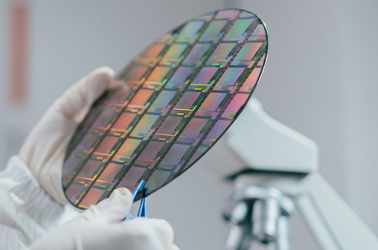
The team applied cryo-ET to recreate polymer structures within a liquid film for manufacturing-compatible lithography, achieving a 99% reduction in residual polymer on 12-inch wafers, according to their publication in the scientific journal Nature on September 30.
Lithography is a critical step in semiconductor fabrication that involves illuminating a photoresist to alter its solubility, then using a developer to wash away the exposed areas, thereby forming specific circuit patterns on silicon wafers.
Peng explained that this innovative approach can be readily adopted in current semiconductor manufacturing processes because it is compatible with existing equipment. He emphasized that industry feedback will be essential for refining the technique and determining future research directions.
The liquid film acts as a vital medium for dissolving the photoresist to produce nanoscale circuit patterns, the team noted. Despite decades of research, the microscopic interactions of photoresist within liquid films and at interfaces remain not fully understood. This knowledge gap has led industry efforts to control pattern defects mainly through trial and error, hindered primarily by a lack of suitable high-resolution imaging technologies.
To overcome this obstacle, the team developed the cryo-ET method to visualize photoresist behaviors in liquid environments. This technique offers high-resolution, three-dimensional reconstructions of the interfacial distribution of photoresist polymers while preserving their native structures during imaging. It allows for detailed observation of polymer chain entanglements within the photoresist.
The global market for photoresists used in semiconductor manufacturing surpassed $2.7 billion last year and is projected to reach approximately $4.5 billion by 2031, according to QY Research. Major industry players include companies based in Japan, the United States, and South Korea, such as Tokyo Ohka Kogyo, JSR, and Shin-Etsu Chemical. Meanwhile, Chinese firms have made inroads in the sector with mid- to low-end products.
Although China faces restrictions on importing advanced lithography equipment, the domestic industry remains committed to developing high-end products, such as extreme ultraviolet (EUV) photoresists, to narrow the gap with international competitors, Peng stated.