Select Language:
August 20 — Lingang Special Area, a central testing ground for economic and trade policies within the Shanghai Free Trade Zone, has become a hub for cutting-edge technology projects. Yesterday’s five new investments pushed the total capital injected into the area since its launch six years ago to CNY 730 billion (USD 101.6 billion).
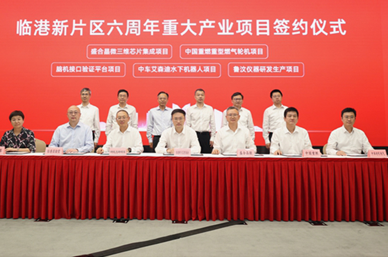
Over the past six years, Lingang has drawn 679 large-scale high-tech projects. The area’s governing committee shared this data at a signing event celebrating its sixth anniversary, during which five major industrial projects with a combined investment exceeding CNY 40 billion (USD 5.6 billion) were announced.
The new initiatives include projects focused on advanced chip packaging, heavy-duty gas turbines, a pilot brain-computer interface testing platform, underwater robotics, and research, development, and manufacturing of integrated circuit equipment.
Launching these advanced chip packaging and IC equipment projects is expected to bolster Lingang’s and Shanghai’s roles as key centers of the integrated circuit industry, explained Li Xiangcong, director of the high-tech division of the governing committee.
“Lingang’s greatest strength lies in its ecosystem,” he emphasized. “The growth of emerging sectors depends on a robust industrial ecosystem, affordable entrepreneurial infrastructure, and access to venture capital.”
Li noted that these latest projects are vital for fostering technological innovation and positioning Lingang for future industries. Particularly, the brain-chip platform aims to support the development of more innovative startups in the region.
SJ Semiconductor Jiangyin, the company behind the advanced chip packaging project, is the first pure-play foundry on the Chinese mainland to combine front-end-of-line manufacturing with high-quality systems.
Vice President Zhou Yan explained that SJSemi chose Lingang because of its advanced core technologies, which will facilitate their research, development, and industrialization efforts. Zhou added that the project will likely become a cornerstone of the company’s business for the next five to ten years or more.
SJSemi is the only Chinese firm utilizing “2.5D” chip packaging technology—an innovative method that integrates multiple semiconductors like computing, storage, and I/O chips into a single package during mass production. This technique boosts performance and minimizes size, operating between traditional 2D and fully 3D stacking methods.
Zhou elaborated that SJSemi’s Lingang project will utilize 3D technology to assemble different types of chips, significantly increasing connection density and enhancing overall performance.
Such high-performance chips are crucial for applications demanding intense computing power, including AI and automotive electronics. Zhou emphasized that moving toward 3D packaging unlocks more business opportunities for SJSemi in Lingang.
She added that Lingang’s strong business environment and well-developed supply chain—both upstream and downstream—make it easier for SJSemi to partner along the industry chain.