Select Language:
Nikon has made a significant leap in semiconductor manufacturing with the announcement of the world’s first maskless lithography system designed specifically for semiconductor backend processes. The new technology, named DSP-100, was unveiled on July 23 and is now available for global pre-orders, with an official release expected by March 31, 2026.
The DSP-100 boasts several core advantages, including high precision, large format capabilities, and increased efficiency. It aims to support the rapidly evolving Fan-Out Panel Level Packaging (FOPLP) technology, which is becoming essential for advanced semiconductor packaging.
By integrating multiple optical lenses from flat panel display (FPD) exposure technology with high-resolution semiconductor processes, the DSP-100 achieves a linewidth/space (L/S) resolution of 1.0μm (1000nm) and a positional accuracy of ≤±0.3μm. This not only enhances image clarity and expands exposure capabilities but also boosts production efficiency by approximately 30%.
Unlike traditional photolithography machines, the DSP-100 employs Spatial Light Modulator (SLM) technology, allowing for direct projection of circuit patterns onto substrates without the need for masks. This innovative approach eliminates the limitations associated with mask size, significantly reduces development and production costs, and shortens product design and manufacturing cycles. Additionally, the absence of a mask minimizes optical distortion, further improving imaging quality.
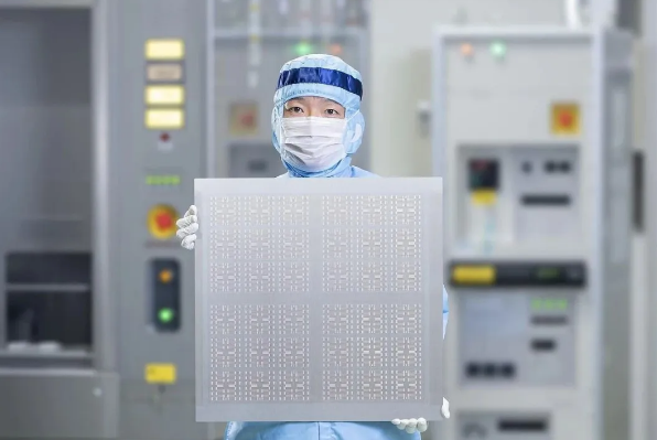
The DSP-100 accommodates substrates up to 600mm x 600mm, catering to the growing demand for FOPLP technology, a prominent trend in advanced packaging. This larger substrate size greatly enhances yield, achieving up to nine times the efficiency when packaging 100mm square chips compared to traditional 300mm wafers.
Testing results have indicated that the system can process up to 50 wafers per hour on a 510mm x 515mm substrate, far exceeding existing wafer-level packaging solutions, with overall production efficiency seeing an increase of around 30%.
As demand for AI chips grows at an average annual rate of 35%, the advanced packaging market is expanding rapidly, with a compound growth rate of 20%. Major industry players such as TSMC, Intel, and Samsung are increasingly adopting FOPLP technology to surpass the limitations of 300mm wafers. The introduction of the DSP-100 provides essential advanced equipment for this burgeoning market.
Nikon has reported interest from several leading packaging companies, and it anticipates that the DSP-100 will capture 20% of the FOPLP equipment market following its launch in the 2026 fiscal year, playing a vital role in the advancement of packaging technology.